Our foundation

Monolithic 3D Integration

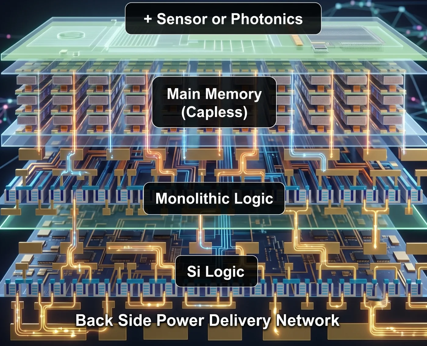
SIM Lab is rooted in a single conviction: the next leap in computing performance will not come from shrinking transistors alone, but from stacking them — logic on memory, tier on tier, grown directly and seamlessly rather than bonded together. We develop the materials, growth techniques, and device architectures needed to make that vision real.

Tap a tier above to jump to the research pillar behind it.

Three directions, one root

Research Pillars

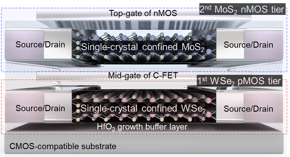
Schematic of a monolithically stacked 2D CFET with MoS2 and WSe2 gate-all-around channels
01

Future Logic Devices

Pushing logic scaling past the limits of silicon with atomically thin, single-crystal 2D semiconductors — wafer-scale 2D GAAFETs and monolithically stacked CFETs that pack more transistors per footprint without sacrificing electrostatic control.
  • 2D GAAFET
  • Monolithic CFET
  • Wafer-scale MoS₂ / WSe₂
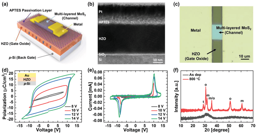
Cross-section and polarization hysteresis of a 2D-channel HZO ferroelectric FeFET memory device
02

Future Memory Devices

Building non-volatile memory that can live directly on top of logic — ferroelectric FeFETs and oxide-based memory cells combining 2D channels with HfO₂-based ferroelectrics for dense, low-power, back-end-compatible storage.

  • FeFET
  • HZO ferroelectrics
  • Back-end-compatible memory
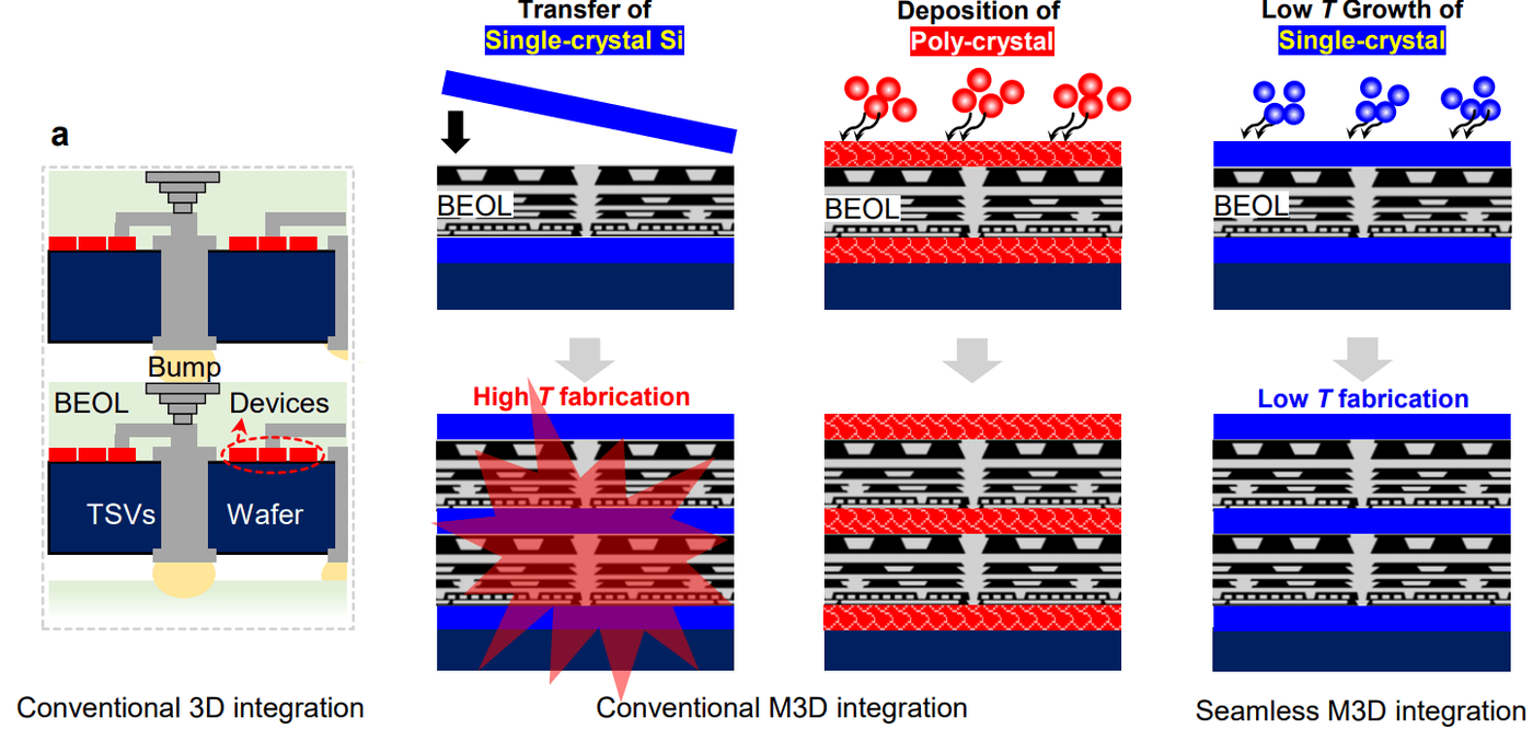
Comparison of conventional high-temperature 3D integration versus seamless low-temperature single-crystal growth
03

Low-Temperature Growth

The enabling technology behind it all: growing single-crystal 2D materials and metals directly on finished circuits, below the thermal budget that would damage them — including laser-assisted and microwave-assisted CVD.

  • Laser-assisted CVD
  • Microwave-assisted growth
  • <400°C single-crystal synthesis

Curious about the details?

See the papers behind these three pillars, or reach out about joining the lab.